
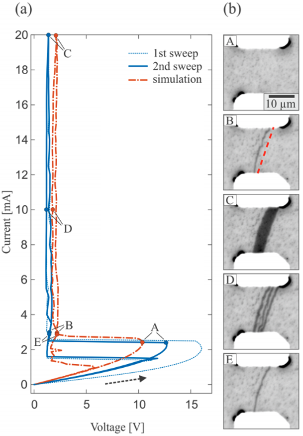
The effect of micro-strain on the switching process in Mott insulators thin film devices. We have used high-resolution cryogenic optical imaging of the electrical switching process in a V2O3 device to find a surprising effect of micro-strain on the filament configuration and the resulting I-V characteristics. (a) Measured (blue curves) and simulated (red curve) current-voltage characteristics. The dashed black arrow indicates the sweep direction. (b) Series of optical microscope images acquired during the second current sweep. As the metallic filament forms, a large reduction in sample resistance is observed (point B). The filament grows with increasing current (C). During the decreasing current ramp the filament splits (D), instead of contracting from the sides as expected from simple thermal considerations. This unexpected behavior, along with the slanted filament geometry can only be explained by considering strain minimization. The profound impact of strain on these out-of-equilibrium phenomena may be harnessed for tailoring resistive switching properties.
See: “Direct visualization of electro-thermal filament formation in a Mott system” – Lange M, Guenon S, Kalcheim Y et al. (2021) – arXiv:2009.12536v1